
Hey it's been a while since I have been able to get back to this problem, but I wanted to provide everyone an update on where things stand. In my case I don't believe that I have a connector problem but rather a noise problem due to the unregulated voltage being sent down to the DSP board.
One of the things that I've done since I last posted was to turn an unused laptop into a primitive scope using the software available on the net plus a circuit buffer board. I wouldn't want to try to take precise measurements with this rig, but it at least offers some insights as to what is going on.
If you look at the schematic, there is a rectifier circuit built around 1000uf C64 that sends unregulated DC down to pin 4 of the connector on the DSP board. Once it arrives there it goes to a LM117 voltage regulator that outputs 3.3 V for the digital circuitry. This regulator has a typical 65dB rejection ratio if no adjustment capacitor is used. I can't really tell what components they have tied to the regulator and haven't tried to figure it out yet.
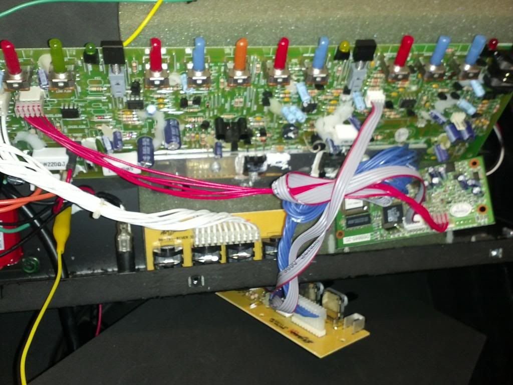
To show you the big picture, the red wires that are about 10 inches long run from the main amp board to the DSP board:
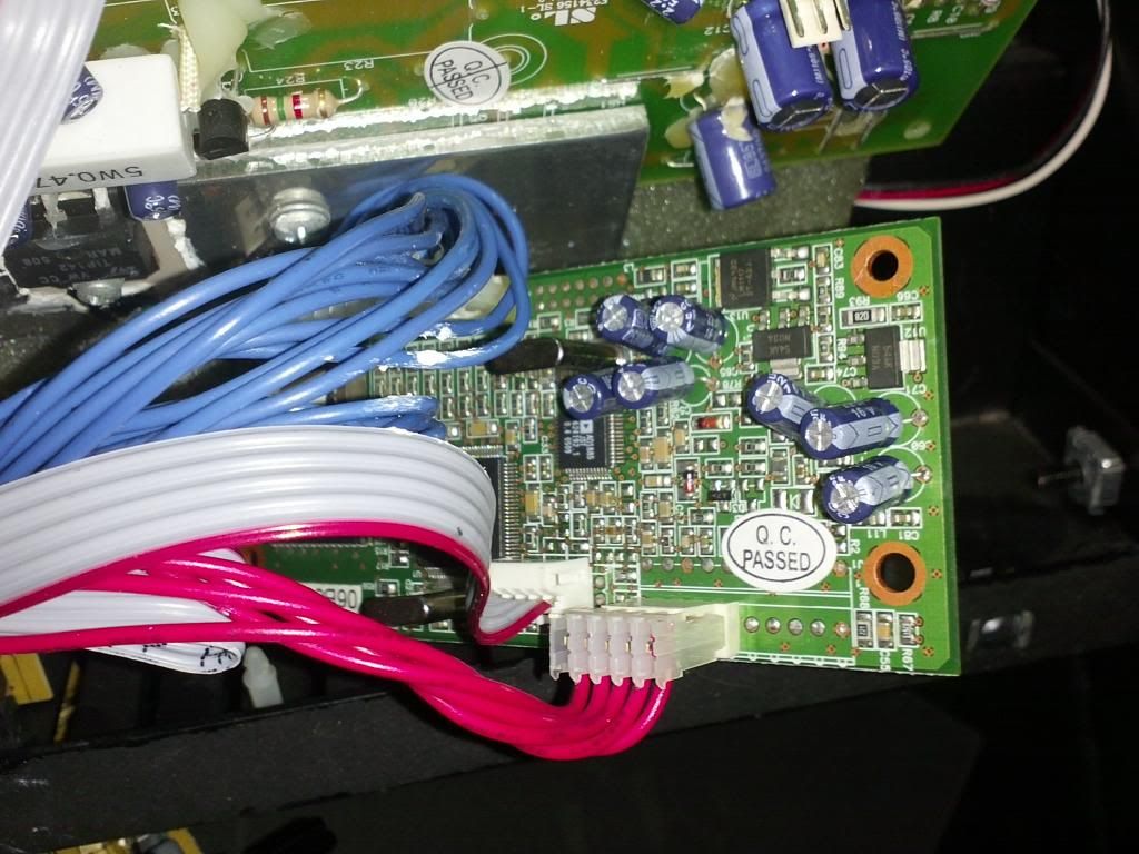
And here is picture of this multi-plane very dense SMD digital board:
So what I am seeing on my "scope" is about 1 Vpp 120 Hz ripple arriving on the DSP board DC input and going to the voltage regulator. This is producing a noticeable 120 Hz hum being being present all the time coming out of the amp because of the DSP output always being mixed in. This equates to a flat low-B humming out of the amp and what has been driving me crazy enough to try to do something about it.
One thing that I found that noticeably reduced the hum was to add a 4700uf capacitor across C64. This gets the ripple down into the .200-.300 Vpp range and seems to get the hum down to a tolerable range where just the broadband type of noise coming from the DSP board is more present.
This looks like it might be a good solution in replacing C64 but one thing I'm not sure about is the purpose of the other circuit that C64 feeds. If you look at the schematic to Q31 and Q16, I think what is going on there is that this is supposed to effectively ground the input to the power amp when the power is turned off to kill wacky artifact sounds as everything fades out. I may be totally off on that so I was hoping someone else here could comment on the intent of that circuit.
One other thing that I tried was to physically separate the red wires going to pins 1 and 2 on J10 from the wire going to pin 4 as much as I could. I was thinking that perhaps there is some significant noise coupling going on along the 10 inch run of unshielded red wires, but I can't say that this made a noticeable difference. I was thinking that running shielded wire with the shield grounded on one end for the audio signals might help here, but I'm not convinced at this point that it would be worth the trouble.
The other idea I was toying with is to add either a pot or a switch between J10 pin 1 and R92 to ground the DSP output (maybe jumper wire JOW1 is the ideal spot) so that when I just want to get the amp as quiet as possible and use external effects, I kill the DSP board output signal. This would still leave the capability to turn the internal DSP back on when the situation allows it.
Years ago I had some experiences dealing with RF noise and personal computer digital communication equipment and even though we had lots of theories on suppressing things, it always seemed to turn into a long tedious trial and error process to find the right combination of things to pass the interference tests. I know this is an audio circuit with much lower frequencies but I tend to think this could also waste a lot of time with diminishing returns trying to do too much with what is probably just a noisy DSP board to begin with.
Any thoughts?
One of the things that I've done since I last posted was to turn an unused laptop into a primitive scope using the software available on the net plus a circuit buffer board. I wouldn't want to try to take precise measurements with this rig, but it at least offers some insights as to what is going on.
If you look at the schematic, there is a rectifier circuit built around 1000uf C64 that sends unregulated DC down to pin 4 of the connector on the DSP board. Once it arrives there it goes to a LM117 voltage regulator that outputs 3.3 V for the digital circuitry. This regulator has a typical 65dB rejection ratio if no adjustment capacitor is used. I can't really tell what components they have tied to the regulator and haven't tried to figure it out yet.
To show you the big picture, the red wires that are about 10 inches long run from the main amp board to the DSP board:
And here is picture of this multi-plane very dense SMD digital board:
So what I am seeing on my "scope" is about 1 Vpp 120 Hz ripple arriving on the DSP board DC input and going to the voltage regulator. This is producing a noticeable 120 Hz hum being being present all the time coming out of the amp because of the DSP output always being mixed in. This equates to a flat low-B humming out of the amp and what has been driving me crazy enough to try to do something about it.
One thing that I found that noticeably reduced the hum was to add a 4700uf capacitor across C64. This gets the ripple down into the .200-.300 Vpp range and seems to get the hum down to a tolerable range where just the broadband type of noise coming from the DSP board is more present.
This looks like it might be a good solution in replacing C64 but one thing I'm not sure about is the purpose of the other circuit that C64 feeds. If you look at the schematic to Q31 and Q16, I think what is going on there is that this is supposed to effectively ground the input to the power amp when the power is turned off to kill wacky artifact sounds as everything fades out. I may be totally off on that so I was hoping someone else here could comment on the intent of that circuit.
One other thing that I tried was to physically separate the red wires going to pins 1 and 2 on J10 from the wire going to pin 4 as much as I could. I was thinking that perhaps there is some significant noise coupling going on along the 10 inch run of unshielded red wires, but I can't say that this made a noticeable difference. I was thinking that running shielded wire with the shield grounded on one end for the audio signals might help here, but I'm not convinced at this point that it would be worth the trouble.
The other idea I was toying with is to add either a pot or a switch between J10 pin 1 and R92 to ground the DSP output (maybe jumper wire JOW1 is the ideal spot) so that when I just want to get the amp as quiet as possible and use external effects, I kill the DSP board output signal. This would still leave the capability to turn the internal DSP back on when the situation allows it.
Years ago I had some experiences dealing with RF noise and personal computer digital communication equipment and even though we had lots of theories on suppressing things, it always seemed to turn into a long tedious trial and error process to find the right combination of things to pass the interference tests. I know this is an audio circuit with much lower frequencies but I tend to think this could also waste a lot of time with diminishing returns trying to do too much with what is probably just a noisy DSP board to begin with.
Any thoughts?
 Unplugging the audio ribbon to the FX board made no difference in my case.


